Previously the network operators intentionally did bother with encryption. This pushed network operators to use it. The world got more secure.
While better than nothing, this encryption was proprietary. The public could not audit it. Historically when the algorithm was not disclosed it was often found to be weak (such as A5/1 in GSM).
In 2023 Midnight Blue released their fantastic work on reverse engineering the TETRA encryption algorithms. They published an implementation of TEA1-4 and also found deliberate weakening of the TEA1 protocol.
So at the turn of 2025/2026 i have released an experimental version of my software which can monitor encrypted calls on a TETRA network. This is of course only if you know the encryption keys (see below on how to obtain them). Also i added support for the reduced keys for TEA1. And also released software to recover the reduced key from on-air traffic.
Hope this will further push operators to step up their security.
Installation and use
The installation is the same as in case of mainline telive and companion software.
Install the telive software from here: GitHub – sq5bpf/telive-2: Tetra live monitor – experimental version using the script in scripts/install_telive.sh . best use a cleanly installed Debian 12.
Try it with an rtl-sdr dongle on an unencrypted network (just like you would use regulat telive), verify that it works with a 1 channel receiver.
Using it to decrypt calls
First of all ask the owner of the network for permission before doing anything with it.
Ask the network owner to give you the encryption key.
This can be tricky because often the key is generated in a keyloader device, which is then used to load it onto base stations and radios. The key never leaves the device in plaintext form.
Please search online forums for info how to obtain this key. A key can be manually entered into the keyloader and then loaded onto the devices.
See below for how to test TEA1 weakness.
Make a backup of sample_keyfile. Edit it to add the network parameters and key.
Start receiver1udp again and see of calls are being decrypted.
Testing TEA1 weakness
As always ask the network owner for permission.
For testing TEA1 weakness, please ask the network owner to temporarily change the encryption to TEA1 (because for sure it is using a stronger algorithm, the vulnerabilities are publicly known since 2023).
I have released TEAtime – software which can be used to recover the short 32 bit key. The process is described in detail in the TEAtime software README.md. Remember to always test the recovered key with a few more candidates in verify mode to see if it is really correct.
Enter the network parameters and recovered key (12345678 in this example) into test_keyfile. For key_num use the CCK ID in from the receiver output (42 in this example, but often it’s 0). Example sample_keyfile:
network mcc 0123 mnc 1337 ksg_type 1 security_class 2
key mcc 0123 mnc 1337 addr 00000000 key_type 16 key_num 42 key 12345678000000000000
Run receiver1udp again and see if audio is being heard from telive.
FAQ
Do I have to get permission from the network operator?
Probably yes. Please obey the laws of the country you are in. Also please provide your findings to the network operator and point them to this software so that they can audit their network.
Is my network using TEA1?
Probably no. TEA1 has been deliberately weakened, and the exact details are known since 2023. Competent network operators have upgraded long ago.
You can try to run TEAtime in crack mod on key recovery candidates. And then run it with the recovered key in verify mode on a few more candidates. If the keystream xor ciphertext value is the same, then it may be a TEA1 key.
What encryption is my network using?
Unfortunately this is hard to tell. The network doesn’t transmit this info.
In short:
- if you can get it to decrypt, then the algorithm and parameters are ok
- If it is a goverment network in the EU it should be using TEA2
- If is some other network, it should be migrated to TEA3 or TEA4
Does it run on xxxx (something other that debian 12)?
Probably not without some tweaking, but i will try to add support for other distributions in the future.
I don’t know how to compile/run this?
This is aimed at experienced users only. In the future i might write some better documentation.
So why was this released?
It was released to get feedback from users who are already proficient with linux, telive and tetra, and preferably are testing this on their own network (which they can reconfigure to test different scenarios).
How can I help?
If you own tetra equipment, them please set up a TEA1 network, generate some test traffic in it (voice and SDS), record the bitstream and publish it (anonymously if you want). This way it can be used as test data.
If you find this description unclear, please email me how to improve it.
We are using TEA1, you are undermining out security!
No, you are undermining it. The information about TEA1 weaknesses was released publicly in 2023, this software is released 2.5 years later.
If you did know this, you were knowingly putting your users at risk, also by providing them with a false sense of security.
If you did not know this, then you are not doing cybersecurity due diligence properly. This info was in TCCA and vendor recommendations, conferences, even public media covered this. By skipping due diligence you were knowingly putting your users at risk.
]]>No need to implement any service emulation, we just redirect the connection back to the attacker’s IP on the same port he connected to us, sit back and enjoy the show 
More info here:
]]>The available modules have very lax bandpass filtering. This can be fixed by a simple filter from a tinned still can and some semirigid coax. The construction is based upon the W1GHZ Altoids Tin Filters publication for 901MHz, but tuned a bit lower.

Construction
Please read the original W1GHZ publication, this construction is very similar.
The filter is housed in a steel candy tin, with dimensions very similar to an Altoids candy tin.
The resonators are made out of 53mm of semirigid cable: 55mm of cable was cut, and then 2mm removed to expose the center conductor so that some of it could be pulled from the cable. The center conductors are fed out of the case via 1.5mm holes.
The resonators are 17mm apart from each other and about 8-10mm from the bottom.
The signal is fed to the resonators via SMA sockets, with feedpoint 11mm from ground.

The box is cleaned from rosin using isopropanol, soldered shut, and then tuned via careful pulling of the center conductors, with the center conductors being bent by hand to touch the case. After tuning the center conductors are soldered to the case.

Results
On 868MHz the filter achieves -20.9dB return loss (SWR 1:1.2) and -0.63dB insertion loss. The insertion loss is lower that the author gives in his publication.
The markers below are:
1. 868MHz 2. 853MHz 3. 901MHz 4. 808MHz 5. 934MHz


The measurement was done via a NanoVNA v2 calibrated right before use.
VY 73 DE
Jacek / SQ5BPF
]]>
So let’s see what we can modify in this radio.
The following modifications will be for the uSDX+ (uSDX plus), with the board marked Ver 3.0, but other radios may be similar and similar modifications may apply.
R23 modification
The uSDX has an unpopulated pad marked R23. Solder 100k there. This resistor is used to discharge the capacitor of the filter that provides the bias to the class-E amplifier. Soldering the resistor enhances carrier power control, and as a result makes SSB sound a tiny bit better.
Note: you may have to set PA Bias max to a higher value when this resistor is soldered.

C24 modification
C24 is connected to the MOSI line, which is used also when flashing the MCU via the ISP. Many descriptions say that it should be disconnected while flashing, or disconnected entirely.
We should not disconnect it, because that line goes to the PA jack. But we can solder the 10nF capacitor vertically and solder a piece of wire that will connect it to ground. This wire will be easy to temporarily unsolder if we ever have a need to do it.

It turns out the usbasp programming interface has a low enough output impedance for this not to be a problem, but it might be useful to disconnect it if other programmers are used.
Shielding fix
The uSDX+ is housed in a nice anodized aluminum case. But aluminium oxide is not conductive, so this case doesn’t actually work like a shield. Is this a problem? Maybe no, because the (tr)uSDX transceiver is housed in a plastic case with no shielding. But since we have a nice metal case, might as well use it as shielding.
Scrub the soldermask around the source of the PA fet and around the BNC jack so that a contact can be soldered there. Make a contact from brass strip and bend it so that it will make good contact with the metal case.

Scrub the aluminum oxide layer to expose raw aluminum where the brass strips touch the case.

Adding an SWR meter and a PA power monitor
I’ve detailed the modifications here:
Adding an SWR meter to a chinese uSDX+ transceiver
Adding an INA219 power monitor to a chinese USDX+ transceiver
Demo of both mods:
Tuning the uSDX output network
The class-E amplifiers have to be tuned for best efficiency. Efficiency can either be displayed via the INA219 power monitor mod (shown above), or can be calculated manually:
– Connect a power meter to the uSDX
– Look at the current in RX, this is usually 40-50mA (call this Irx)
– Transmit a carrier in CW
– Assume that the PA current during transmit is Itx-Irx (where Itx is the current during transmit)
– Calculate the input power as Pinput=Vsupply*(Itx-Irx) (Vsupply may be the power supply voltage, or in case of the uSDX+ it is power supply voltage-0.7V where 0.7V is the silicon diode voltage drop)
– Calculate the efficiency as Poutput/Pinput*100%
Doesn’t matter if the efficiency is calculated manually or just shown by the device (which i would recommend), we want to tune for maximum efficiency for each band on the center frequency of the range of frequencies that we will mostly use (center of band, or maybe center of the first 100-200kHz of the band for CW operators)
The tuning procedure is:
– Set the power supply to 12V
– Change the frequency in increments of 100kHz
– If the efficiency is declining with increase of frequency, then increase the inductance of the coil which is connected to the drain. If the efficiency is declining with decrease of frequency, then decrease the inductance of the coil which is connected to the drain. Making the windings closer to each other increases the inductance, spreading them more evenly on the core decreases it.
It is much easier with having the efficiency calculated on the display. Just change the inductance to achieve the best possible efficiency.
I have increased the efficiency of the PA stage to over 70% on the high bands, and more on the low bands. For some this is around 90%.
Increase power by changing the output transistor
The output power depends on the power transistor being used. These are being used:
– 3 * BS170 – this is the usual setup. I have been asked to fix a (tr)uSDX with the PA blown, so guess it’s not that bulletproof
– IRLML2060 – great (and very small) transistor when the matching networks are tuned for the frequency of operation. Unfortunately it will often fail when mismatched, especially in the field. See SV9/SQ5BPF with uSDX part 2
– IRF510/IRF520/IRF530 – these transistors have very big gate capacitance. Also not good on the higher bands.
– IRLL110 – i have tried this transistor based on Pmax and Idmax. Not great on the higher bands, but works great on 20m and below (and probably higher, but then i didn’t have the modified radio o show efficiency).
– FDT86256 – looks like a great fet. The maximum power and current are bigger. If the tuning is good, then this is probably the best output device.
Want more mods for your uSDX version?
I can’t possibly support all uSDX versions and make mods for them, because i don’t have them. If you have an unused uSDX, and would like to see new mods for it, you can donate it. Even a broken one will do if it’s easily fixable (for example PA transistor failure). If you have such a radio, please send email to [email protected]
]]>I have an uSDX+ transceiver from China. Let’s add the power monitor to it too. This description should apply to other radios based on the uSDX.
To make this mod you need some manual and soldering skills, a basic understanding of electronics, and the ability to compile and flash your own firmware through the 6-pin ISP connector. Also the SWR meter mod has to be done first. If you are uncomfortable with this, then just buy an original (tr)uSDX.
We will use a popular INA219 board, avaliable from Adafruit or other manufacturers:

The connections are simple:
– Locate the trace that provides connect the power supply to the PA (power amplifier), cut it, connect VIN+ to the power supply side, VIN- to the PA side
– Connect to the I2C bus from the ATmega328P: PC4 to SDA, PC5 to SCL
– Connect GND to ground. Connect Vcc to +5V. Note: this will make the voltage on the I2C bus higher by 0.13V (1.4V*1k/(1k+10k)), which is not really a problem.
The uSDX+ has these exposed as traces on the underside of the board, for other radios you will have to trace them yourself, and if they are not available on the bottom side then route them from the top side.

Closeup:

The board is thin enough to be placed on the underside of the uSDX+ board:

Software Support
I have added INA219 support to the original uSDX sources. My changes have been incorporated into the original uSDX firmware: https://github.com/threeme3/usdx or you can use my version which may contain some changes/fixes/bugs not yet present in the original firmware: https://github.com/sq5bpf/usdx
Uncomment (remove the // before the #define) the #define SWR_METER 1 line and #define INA219_POWER_METER 1 in the usdx_settings.h file , comment the CAT and DIAG functionality, optionally do some other changes, and recompile in Arduino IDE. If there are no errors, then flash the firmware using the 6-pin ISP conector on the uSDX board (i use a uspasp-compatible programmer for that). After uploading, reset settings if the radio hasn’t done this by itself.
Calibration
The calibration settings provided in the usdx_settings.h are ok for my radio, but this can be calibrated for better accuracy.
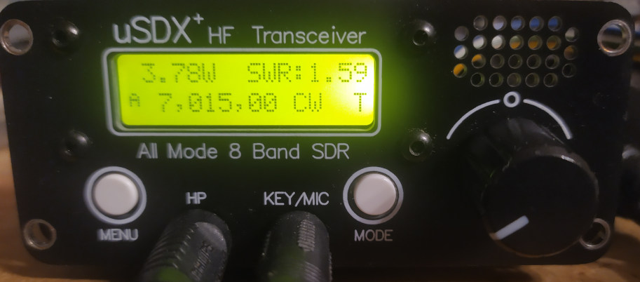
Change the 1.13 SWR Meter option to FWD-SWR, change to CW mode and transmit a constant carrier into a dummy load and power meter. The display should show forward power and SWR:
Change the 1.14 Cal. power menu setting so that the uSDX power meter shows the same power as the external power meter. Preferably do this on one the higher bands.
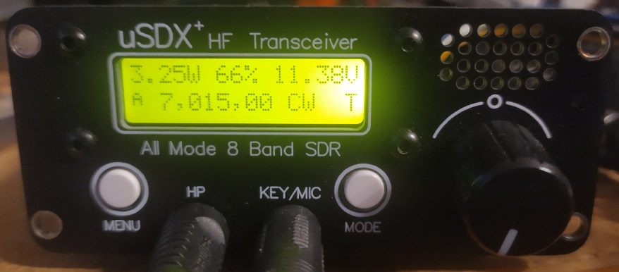
Now break the connection between the power trace and VIN+ and connect an ammeter between the power trace and VIN+. Change the 1.13 SWR Meter option to I-U-P (PA current, voltage, input power) and transmit.
Change the 1.15 Cal. current menu setting so that the uSDX current meter shows the same current as the external current meter:

The above photo shows 3.35W PA input power, 439mA PA current and 11.37V PA voltage.
Change the 1.13 SWR Meter option to PWR-EFF and this should show the output power and PA efficiency ( 100% * PA output power/PA input power).
Using the Power monitor meter
For normal operation set the 1.13 SWR Meter option set to FWD-SWR, which shows the output power and SWR. Other useful options are PWR-EFF which shows the output power and efficiency and I-U-P which shows the input power/current/voltage (useful to estimate battery state in the field).
Substract the output power from the input power to see how much power is wasted in the finals. The BS170 has maximum dissipation of 830mW, there are 3 transistors in parallel, so if the wasted power is over 2.49W (830mW*3) they are operating over maximum specifications and can be quickly destroyed.
A class E PA stage should be tuned for best efficiency. The series inductance (not the lowpass filter/2nd harmonic filter inductance) can be changed to optimize efficiency. Change the frequency in increments of 100kHz. If the efficiency falls with frequency increase, then the series inductance should be higher (bring the windings closer to each other or even add an extra turn if this is not enough). If the efficiency falls with frequency decrease, then the series inductance is too low (spread out the windings more evenly or even remove one turn).
Note: the uSDX+ and other similar 8-band radios don’t have an output circuit for 12m, so it’s better not to optimize for this band.
VY 73
Jacek / SQ5BPF
]]>I have an uSDX+ transceiver from China. Let’s add the SWR meter to it too.
To make this mod you need some manual and soldering skills, a basic understanding of electronics, and the ability to compile and flash your own firmware through the 6-pin ISP connector. If you are uncomfortable with this, then just buy an original (tr)uSDX.
The (tr)uSDX schematics are available at the Manuel DL2MAN site. We can see that the SWR bridge is a Stockton bridge , with a minor twist: while the current transformer is 1:7, the voltage transformer isn’t 1:7, but 3:21. This results in the same transformation ratio, but has a higher impedance so loads the transmitter less. Quite clever.
We can get the bridge schematics from the (tr)uSDX high bands PA board:

The FWD (forward voltage) and RVS (reverse voltage) signals are connected to the ADC6 (FWD) and ADC7 (RVS) pins. These are only present on an SMD ATmega328P MCU, so if you have a radio with the DIL version (such as the DL2MAN sandwich) you can’t perform this mod.
Luckily my uSDX+ radio, and i think all uSDX radios pre-built in china, uses an ATmega328P in the TQFP32 SMD package.
The next obstacle is where to install the bridge. In the uSDX that i have the only place is on the underside of the board near the BNC antenna connector.
So first cut the connection to the BNC connector:

Then drill through the PCB with a 1mm (or smaller) drill bit, being extra careful not to drill through some important trace. Chamfer the hole from both sides with an about 3-4mm drill bit:

Bottom:

Next place a piece of Kynar-type wire through the hole and solder it to the transmitted output trace. Be careful to solder to both sides of the trace, because the drilling has probably cut the trace in half.
Use the soldered Kynar-type wire as the 1-turn winding of the current transformer T1. The rest of the bridge can be easily build in ugly manhattan-style on a piece of perfboard. Note: i used 47k resistors instead of 68k inthe original schematic.

Note: the underside of the transformers and bridge is insulated by black insulating tape. The bridge is also covered by insulating tape after it has been confirmed to work.
Next we need some way to connect the wires to the CPU. The easiest was to drill a 2mm diameter hole in the PCB.

Note: this is dangerous, and you don’t know how many layers this board has, so you might drill through some trace which is not visible. So best avoid what i’ve done and route the wires in some other way.
Next solder two 10nF capacitors between ground and ADC6 and ADC7. Connect the wires from the SWR bridge to the CPU: ADC6 (FWD) and ADC7 (RVS):

The SWR bridge fits nicely in the uSDX+ metal box on the underside of the board (with about 1mm clearance):

Software Support
There was software support for the SWR meter in the original uSDX software, however i have added the ability to calibrate the power meter using the “Cal. power” option in the menu. My changes have been incorporated into the original uSDX firmware: https://github.com/threeme3/usdx or you can use my version which may contain some changes/fixes/bugs not yet present in the original firmware: https://github.com/sq5bpf/usdx
Uncomment (remove the // before the #define) the #define SWR_METER 1 line in the usdx_settings.h file , comment the CAT and DIAG functionality, optionally do some other changes, and recompile in Arduino IDE. If there are no errors, then flash the firmware using the 6-pin ISP conector on the uSDX board (i use a uspasp-compatible programmer for that).
After uploading, reset settings if the radio hasn’t done this by itself, change the 1.13 SWR Meter option to FWD-SWR, change to CW mode and transmit a constant carrier. The display should show forward power and SWR:
If the readout shows very high SWR on a dummy load (or matched antenna) and/or very low forward power, then exchange the connections of one of the four windings on the FT37-43 toroids (doesn’t matter which, use the one which is the easiest to reach).
If you have a power meter and a dummy load, then connect it to the radio, and change the 1.14 Cal. power menu setting so that the uSDX power meter shows the same power as the external power meter. Preferably do this on one the higher bands.
Disclaimer: i am not responsible for anything caused by doing or not doing this modification. If you break your radio, then you’re on your own
VY 73
Jacek / SQ5BPF
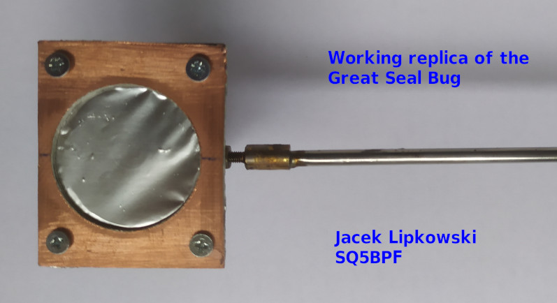
]]>As far as i know this is the only attempt to make a working replica, not only a nicely looking prop.
I am a licensed radio amateur (callsign SQ5BPF), therefore the device dimensions were scaled to make it operate on the amateur radio 23cm band (1240-1300 MHz). Please see my other articles about this device.
]]>
To my knowledge this is the only publication about making a wirking replica of the Sreat Seal Bug. https://www.vintagespycraft.com/ shows a beautifully looking model, however the emphasis was on making it a nice looking exhibit, and not on making it work (but look at this site anyway, the model is a work of art).
In 1945 this was super-secret, ultra-novel military technology. Building and operating it required special materials and access to ultra-secret hardware. So is it possible to do this in 2022 on an amateur budget? Surely not.
But radio amateurs have a long history of doing “impossible” things, part because of their ingenuity, and part because of their ignorance (they simply don’t know something can’t be done). So lets try anyway
The construction of the Great Seal Bug is described in the top secret FBI document “Drawing and Photographs. Russian Resonant Cavity Microphone” [1] from 1952, which was declassified in 2019 (after 67 years):

I will use most of this design, but won’t attempt to make a 100% copy. Instead I will try to make the device from commonly avaliable materials, using commonly avaliable tools. Also it should be as cheap as possible, even if that means sacrificing performance or making it look ugly (and it will!). Also I will try to document my errors.
Choice of frequency
The original design is for 1700 MHz, which was free in 1945, but now is in the uplink frequency range for GSM DCS. Transmitting there would be radio piracy, and also very stupid because the mobile phone companies paid a lot of money to use these frequencies, and therefore actively monitor for interference.
Fortunately I am a licensed radio amateur (my callsign is SQ5BPF), so I can legally use the 23cm amateur radio band (1240-1300 MHz) for my experiments. This is a good choice, because I already have made some equipment for this band, and also the cheap rtl-sdr dongle covers this band.
If I wasn’t licensed I would probably use the 868 MHz or 2.4 GHz ISM bands.
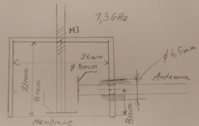
My choice of frequency is 1296MHz, so every dimension has to be multiplied by 1700/1296 = 1.3
The following ugly drawing shows the calculated dimensions.
Choice of materials
I will try to use low-loss materials: copper and brass.
Amateur radio operators have used microwave filters made from copper pipe caps for a long time. They are cheap, simple to make, easy to tune, and forgive a lot of construction errors. These “pipe cap filters” were pioneered in 1988 by Roman Wesołowski DJ6EP (Polish callsign SO3EP and ex SP3GDQ). There are many examples of such filters on the internet (search for “pipe cap filter”), some here:
https://www.wa5vjb.com/references/CheapMicrowaveFilters.pdf
http://w1ghz.org/filter/Pipe-cap_Filters_Revisited.pdf
Naturally i will also use a pipe cap.
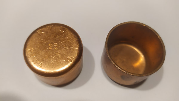
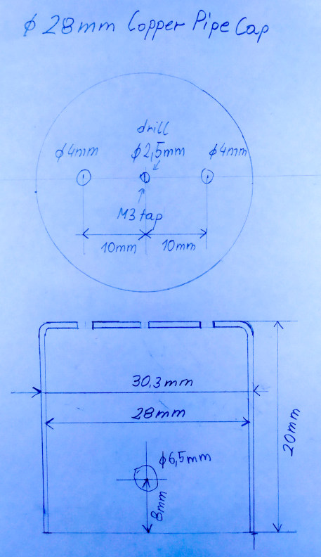
The best pipe cap i could find is a 28mm pipe cap (for 1″ pipes). These have 28mm internal diameter, 30.3mm external diameter and 20mm depth:
Unfortunately this project has some problems, but all are solvable:
- We want 22mm depth, and this has only 20mm. This can be extended by soldering a brass strip on the outside (this will be shown later).
- There is nothing to hold the microphone membrane and provide good good electrical contact with the whole circumference of the cylinder. This will be done with two double-sided copper laminate used for PCBs.
- We need something dielectric with good microwave properties to hold the antenna. Originally it was a special piece of plastic with inside thread. We will just use double-sided FR4 copper laminate.
- It would be nice to be able to try different antenna lengths. We will just use a telescopic antenna.
- Were do we get an ultra-thin silver plated membrane? We’ll just use aluminum foil, the cheapest kinds are very thin. This is not the best choice, but best i had (thin copper foil, preferably silver-plated would be much better).

Preparing the pipe cap
Below is a drawing where the pipe cap should be drilled:
The pipe cap was then cleaned with steel wool and dishwashing detergent.
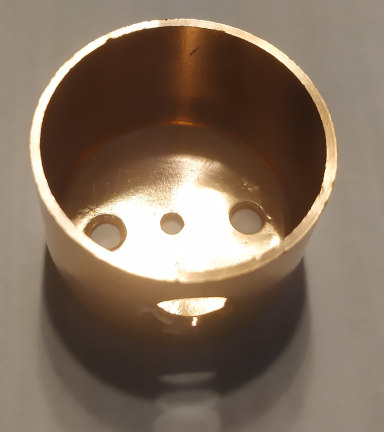
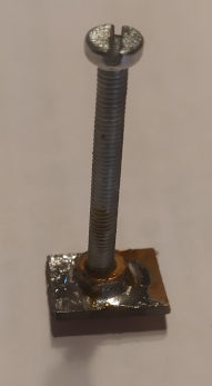
The 2.5 mm hole in the center was tapped with a M3 thread. Next a steel M3 screw with a brass M3 nut is screwed from the outside into this hole, and the brass nut is soldered to the pipe cap. The steel screw is removed after soldering. All soldering of the pipe cap is best done with a high power soldering iron, I used a 300W soldering iron.
The antenna mount is made from a rectangular 10mm x 13mm piece of double sided PCB laminate (FR4), with a 2.5mm hole drilled in the center. The copper around one side of their hole is removed with a very shallow drilling

This 2.5mm hole is tapped with a M3 thread. Next a steel M3 screw with a brass M3 nut is screwed into the hole, and the brass nut is soldered to the copper laminate.
This antenna mount is soldered to the hole on the side of the pipe cap. After soldering excess copper foil around the brass nut is removed with a file. Below is the antenna mount with the internal elements mounted for a test. Check the mount with an ohmmeter, there should be no electrical contact between the antenna and the pipe cap.
A 10mm brass strip, 0.3mm thick, is soldered to the outside of the pipe cap, so that the internal height is 22mm (2mm greater, because pipe cap internal height is 20mm). The brass strip has a rectangular hole cut out so that it doesn’t go over the antenna mount. The area of the pipe cap which is under the brass strip should be tinned before soldering the brass strip. Use a high power soldering iron for this.

Cut and file away the extra brass, so that the outside is round.
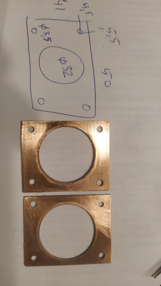
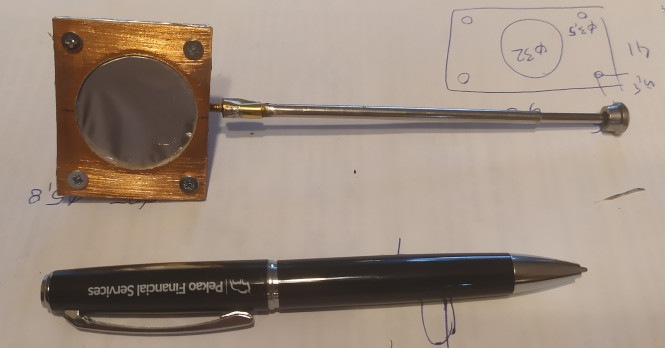
Next make a holder from two rectangular pieces of double-sided PCB board, with 3.5mm holes 5.5mm from the sides, and a 32mm hole in the middle. The two pieces should fit exactly over each other:
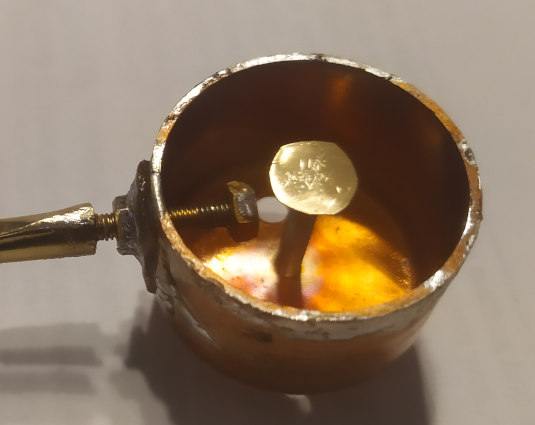
Put the pipe cap into the big hole, so that the brass strip sticks out a bit (around 0.5 – 1mm). Solder the brass strip to the copper PCB.
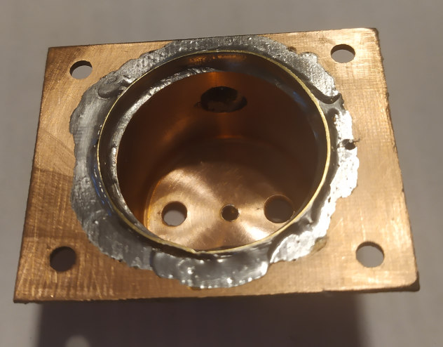


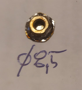
Prepare two brass disks of around 8-9mm diameter, and solder them to brass M3 nuts:
Solder a brass 40mm long M3 screw to a telescopic antenna. The exact method will depend on the antenna type. I made an adapter from a piece of brass strip surrounding the antenna and the screw head.
Now prepare for the final assembly. File away excess solder. Clean everything with steel wool with detergent, wash with water, and then clean with alcohol. If you want to silver-plate the inside of the pipe cap, the screws and the capacitance disks, you can do so now (and after silver-plating wash with water and alcohol again).
The tuning screw is a 45mm brass screw. I also added two washers, a spring (from a ball-point pen), and some nuts at the end.

A potentiometer knob can be mounted on the nuts at the end of the screw:
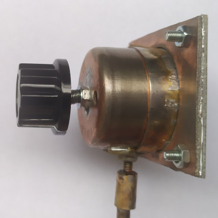
Assemble everyting inside:

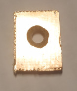
Install the thin foil membrane. I used cheap aluminium foil here (usually the cheaper foils are thinner), silver side to the pipe cap. Try to have the foil as straight as possible. Put the other PCB laminate holder on it, and screw the two together with M3 screws.

And cut away the extra foil:
Congratulations! You’ve just built a russian top-secret cold-war passive microphone.
But does it work? There is only one way to find out (in the next article).
Author: Jacek Lipkowski SQ5BPF
Literature:
[1] https://www.cryptomuseum.com/covert/bugs/thing/files/GREAT_SEAL_BUG.pdf
]]>This part is a short explanation the theory of operation.
The FBI has unclassified the initial report about the Great Seal Bug [3]. It has a lot of construction details, including most dimensions:
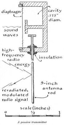
The “great Seal Bug” is a resonant circuit made from distributed elements. The following diagram shows a simple lumped element resonant circuit, and a distributed element resonant circuit (with the distributed capacitance and inductance shown in blue):

Such a distributed element circuit can have very low losses, and therefore a high Q factor. Most losses are due to resistive losses and the skin effect, these losses can be made very low by using thick conductors (lots of surface area) and low resistive loss material (copper, preferably silver plated for even lower loss).
The Great Seal Bug consists of a metal cylinder, with a metal rod inside, this is the resonant circuit. One side of the can is a conductive membrane, which is used as a microphone membrane. An antenna is capacitively coupled to this resonant circuit.
The capacitance between the membrane and the rod in the center of the bug varies with the membrane position (which is moved by sound). Changes in the capacitance vary the resonant frequency of the circuit.
A N * 1/2 wavelength antenna is capacitively coupled to the resonant circuit (the designers of the Great Seal Bug used N=3, so the antenna was 3/2 wavelengths long). Such antennas have very high input impedance, and thus don’t need a big counterpoise, the metal cylinder is more than adequate.

This antenna is “illuminated” by a carrier wave from a radio transmitter on a frequency near the resonance frequency of the tuned circuit. Some portion of this energy is re-radiated from the antenna. The amount of the re-radiated energy depends on the impedance presented by the tuned circuit. This impedance changes by a large amount, because this circuit is near resonance.
So the method of operation is as follows:
- As the metallic membrane vibrates, it changes distance from the inner rod.
- This change in distance causes a change of capacitance to the inner rod.
- The change of capacitance changes the resonant frequency of the tuned circuit.
- This causes great changes to the impedance of this tuned circuit at the “illumination frequency”.
- Changes to this impedance vary the amount of the re-radiated radio wave
- The result can be seen as AM (amplitude modulation) and some PM (phase modulation) of the re-radiated radio wave. In practice only the AM component is used.
This leads to the following design principles:
- The distance from the metal membrane to the inner rod should be very small, because this results in the biggest capacitance changes when the membrane is vibrated. According to [1] the distance was 0.23mm.
- The electrical properties (impedance) at the illumination frequency of the tuned circuit should vary greatly when the resonant frequency changes. So this needs to have a high Q. High Q can be achieved when low loss materials are used, so preferably the elements (including the inner side of the membrane) should be silver-plated.
- The membrane should move as freely as possible, so it should be very thin (6.35um according to [1]). Also the metal cylinder should have a hole on the back side, so that the membrane is not damped by an air cushion.
This device is has a lot of advantages to the eavesdropper:
- No power supply is needed, so the device can work forever.
- Low probability of detection using 1950’s technology. When there is no illumination signal, not signals are transmitted back
- Low probability of detection using 1970’s technology – the non-linear junction detector, because there are absolutely no semiconductors inside [2]
Author: Jacek Lipkowski SQ5BPF
Literature:
[1] https://www.cryptomuseum.com/covert/bugs/thing/
[2] https://en.wikipedia.org/wiki/Nonlinear_junction_detector
[3] https://www.cryptomuseum.com/covert/bugs/thing/files/GREAT_SEAL_BUG.pdf
]]>This device, even 75 years later, is still often mentioned at security publications and conferences.

On 4 August 1945, at the end of WW II, the Pioneer scouts (children from the Pioneer Organization of the Soviet Union) gave Averell Harriman, the USA ambassador, a beautiful wooden replica of the Great Seal of the United States. This was a “gesture of friendship” to USA, USSR’s war ally.
This replica was hung in the conference room in the residence of the US Ambassador in Moscow.
According to different accounts, the US learned around 1951-1952 that a listening device has been planted at the ambassador’s residence. There are two main versions circulating: in 1951 the British altered the Americans that a listening device is active, in 1952 the Americans found the bug themselves. Espionage and counterespionage are difficult subjects, and many other versions also could be possible, including the possibility that the bug was left on purpose to feed misinformation to the eavesdroppers.
It was found that the seal contained a novel passive microphone. The microphone was mounted in the inside of the wooden carving, with small holes under the eagle’s beak to pass the sound.

The bug consisted of an antenna coupled to a microwave distributed element resonator, part of which was a flexible microphone membrane. This is irradiated by a carrier at the resonant frequency of the resonator, which is picked up by the antenna, and then re-radiated. The resonant frequency of the resonator is very dependent on the membrane position, so when the membrane moves it changes the amount of re-radiated carrier signal, resulting in AM and PM modulation of the re-radiated signal. The working frequency was about 1.7-1.8GHz.
On May 26, 1960 the bug was presented at the United Nations Security Council to show that the US was constantly being targeted by eavesdropping by the USSR.

A detailed drawing of “The Thing” was published in the March 1968 edition of Scientific American:
The bug was designed by Leonid Theremin , inventor of the theremin instrument . [6]
In 2019 the FBI unclassified a detailed report about “The Thing” from 1952. This report contains detailed drawings of this device, with dimensions [2]. It is avaliable at this link: https://www.cryptomuseum.com/covert/bugs/thing/files/GREAT_SEAL_BUG.pdf
A lot of information about this device and it’s history, including information not published elsewhere, is published by Murray Associates in [4]
Author: Jacek Lipkowski SQ5BPF
Literature:
[1] https://www.cryptomuseum.com/covert/bugs/thing/
[2] https://www.cryptomuseum.com/covert/bugs/thing/files/GREAT_SEAL_BUG.pdf
[3] https://counterespionage.com/great-seal-bug-part-1/ https://counterespionage.com/great-seal-bug-part-2/ https://counterespionage.com/great-seal-bug-part-3/ https://counterespionage.com/great-seal-bug-part-4/ https://counterespionage.com/great-seal-bug-part-5/
[4] https://en.wikipedia.org/wiki/The_Thing_(listening_device)
[5] https://hackaday.com/2015/12/08/theremins-bug/
[6] https://en.wikipedia.org/wiki/Leon_Theremin
]]>